
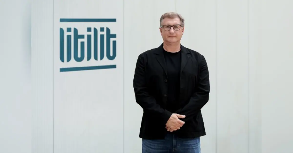
Lithuanian laser manufacturer LITILIT stated that femtosecond lasers are becoming vital instruments to resolve precision bottlenecks in advanced computing hardware. As artificial intelligence models expand in complexity, providers face serious physical hurdles when turning capital into functioning chips and components. According to research firm Gartner, companies will spend nearly $1 trillion on infrastructure for artificial intelligence this year, followed by an additional $6 trillion between 2027 and 2030.
The Manufacturing Barrier in Modern Computing
Building physical hardware for data centers involves processing materials at microscopic tolerances. Components require structural features thinner than a human hair, where traditional mechanical equipment tends to crack or chip materials. Nikolajus Gavrilinas, chief executive and co-founder of LITILIT, noted that hardware production requires precision levels that conventional industrial tools struggle to provide consistently.
“The brain of AI was built in software labs. Its body is being built on factory floors, one microscopic hole and one crack-free cut at a time, and how fast AI grows from here depends on how quickly precision manufacturing can scale.”
Nikolajus Gavrilinas, CEO and Co-Founder of LITILIT
Through-Glass Vias and Precision Engineering
A primary bottleneck in modern fabrication involves through-glass vias, which are vertical micro-holes drilled through glass to transmit electrical signals. Mechanical drilling often causes uneven hole dimensions and structural micro-cracks across substrates. Industry tracker TrendForce does not expect glass core substrates to reach commercial volume production until after 2030 as a result of these fabrication hurdles.
To solve this challenge, specialized industrial lasers fire light pulses lasting one quadrillionth of a second. This rapid pulse removes material before thermal energy can spread into surrounding glass panels. Consequently, operators can create thousands of uniform openings across substrate sheets without melting edges or inducing fractures in underlying silicon layers.
Applications of Femtosecond Lasers Across Hardware
High bandwidth memory architectures require stacking 12 to 16 individual chips that are thinned down to tens of micrometers. Traditional mechanical saws frequently damage these delicate stacks. In contrast, modern optical tools slice fragile wafers cleanly while maintaining structural integrity across delicate layers of computers and high-density memory packages.
Circuit boards designed for advanced processors also rely on hard materials that rapidly degrade traditional mechanical drill bits. Optical tools shape these rigid boards and etch fluid cooling channels directly into silicon, ensuring stable thermal management. Furthermore, the technology aids consumer hardware, cutting crack-free cover glass and camera lenses for modern mobile devices running local neural models.
Scaling Industrial Laser Production
Most short-pulse systems originated as scientific laboratory instruments and historically lacked designs suitable for high-volume manufacturing. LITILIT addressed this bottleneck by securing two patents, including one created with Lithuania’s Center for Physical Sciences and Technology. Specifically, the modular architecture reduces component complexity and automates assembly lines. As a result, the company plans to produce 3,000 femtosecond lasers annually at full capacity inside its factory in Vilnius.